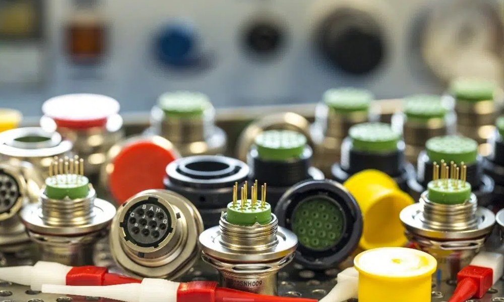
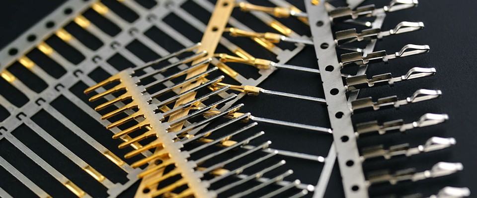
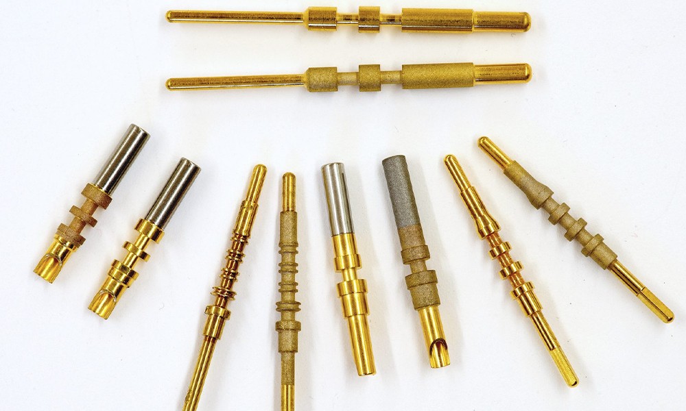
In the manufacturing of connector contact parts—such as pins and sockets—the quality of the metal plating plays a decisive role in electrical performance and long-term environmental reliability. Industry failure analysis reports show that up to 28% of connector failures are directly caused by improper plating thickness or poor plating uniformity, and 90% of early failures (within 6 months) can be traced back to plating defects.
Insufficient plating thickness accelerates wear and corrosion, while excessive thickness may cause brittleness and cracking. Poor uniformity creates localized weak points that become failure hotspots. This article explains, from the perspectives of electrochemistry, contact mechanics and environmental durability, why strict control of plating thickness and uniformity is essential for high-reliability connectors.
1. Functions of Plating on Connector Contact Parts
1.1 Multiple Technical Roles of Plating
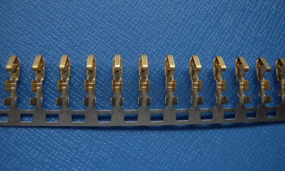
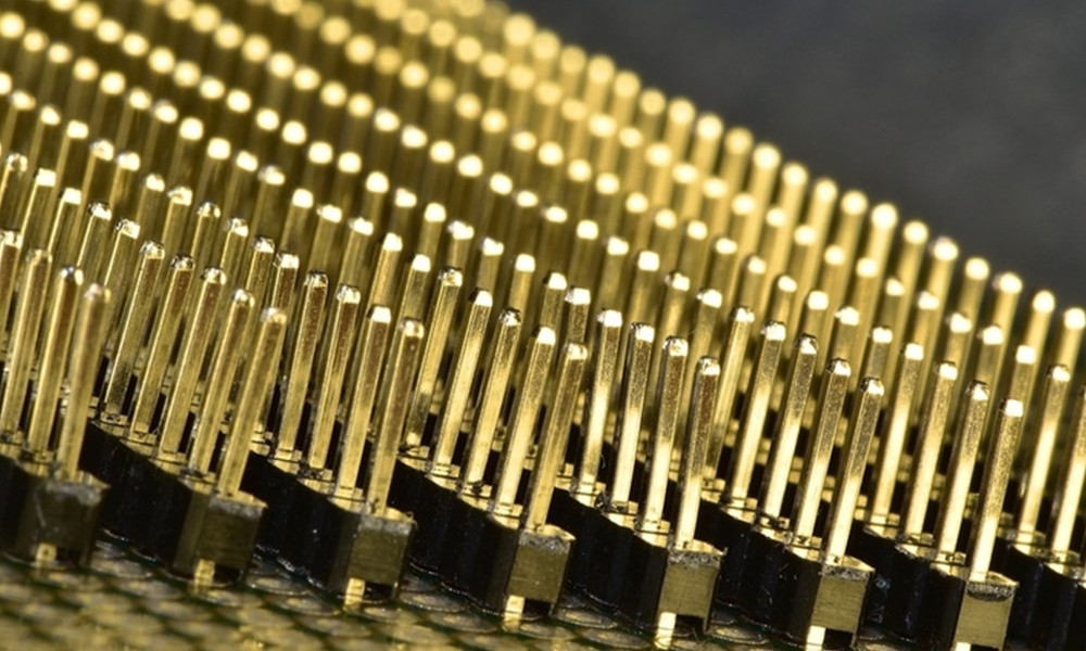
Plating materials such as gold, silver and nickel provide three key functions:
1) Reduction of Contact Resistance
Gold and silver have extremely low resistivity (Au: 2.4 μΩ·cm, Ag: 1.6 μΩ·cm).
A proper gold plating layer allows connectors to maintain <10 mΩ contact resistance, far lower than oxidized copper alloy surfaces (~17 μΩ·cm).
2) Corrosion Protection
The plated layer forms a barrier that prevents copper or steel substrates from reacting with oxygen, moisture and salts.
In salt-spray environments, a qualified gold plating layer can reduce corrosion rate from 0.1 μm/day (bare copper) to <0.001 μm/day.
3) Reduced Friction and Wear
Gold plating has a low friction coefficient (μ ≤ 0.3), lowering wear during repeated mating cycles.
For example:
A hard gold-plated connector shows <0.5 μm wear after 5000 cycles
A non-plated copper contact may wear up to 5 μm
1.2 Industry Standards for Plating Thickness and Uniformity
Different applications require different plating systems. Typical standards:
| Application | Plating Type | Gold Thickness | Uniformity (Thickness Variation) | Porosity Requirement |
|---|---|---|---|---|
| Consumer Electronics | Gold/Nickel | 0.5–1 μm | ≤ ±20% | ≤ 1 pore/cm² |
| Industrial Controls | Gold/Nickel | 1–3 μm | ≤ ±15% | ≤ 0.5 pores/cm² |
| Automotive Electronics | Gold/Silver/Nickel | 2–5 μm | ≤ ±10% | No visible pores |
| Aerospace | Hard Gold/Nickel | 5–10 μm | ≤ ±5% | Zero porosity |
Nickel underlayers (2–5 μm) improve adhesion and block copper diffusion.
2. Risks of Incorrect Plating Thickness
2.1 When Plating is Too Thin
1) Accelerated Wear and Substrate Exposure
A gold layer thinner than required wears rapidly under mating cycles.
Testing example:
0.3 μm gold → copper substrate exposed after 1000 cycles, resistance rose from 8 mΩ → 50 mΩ
2 μm gold → resistance increased only to 12 mΩ
Exposed copper oxidizes within 24 hours, drastically degrading conductivity.
2) Loss of Corrosion Protection
Thin plating increases porosity (>5 pores/cm²).
In humidity (60°C / 90% RH), corrosion products (CuO, Cu₂O, malachite) expand and cause blistering and peeling, leading to complete failure within months.
2.2 When Plating is Too Thick
1) Brittle Layer and Cracking
Gold thickness >10 μm increases internal stress dramatically:
1 μm → ~50 MPa
10 μm → ~200 MPa
During temperature cycling (−40°C to +125°C), excessive thickness leads to cracking.
Example:
Aerospace connector with 15 μm gold cracked after 50 thermal cycles, failing salt-spray test in 72 hours.
2) Dimensional Tolerance Issues
Plating adds material to the contact surface.
For 0.8 mm pitch connectors, a 0.02 mm plating overshoot can cause excessive insertion force or jamming.
3. Risks of Poor Plating Uniformity
3.1 Local Thin Areas Become Weak Points
1) Electrical Hotspots and Overheating
Uneven plating causes current to flow more heavily through thicker regions, leaving thin areas to overheat.
Example:
An EV high-voltage connector (250 A load) had a corner plated at only 50% of target (1 μm vs. 2 μm).
After 3 hours of operation, the local temperature reached 120°C, exceeding insulation limits (105°C).
2) Corrosion Initiation Sites
Thin areas corrode 5–10× faster.
Marine-grade connectors with local thin plating failed within 6 months due to pitting corrosion.
3.2 Process Defects Trigger Secondary Failures
1) Reduced Adhesion
Non-uniform plating often correlates with overly fast local deposition, resulting in poor adhesion.
Uniform layers reach ISO 2409 adhesion level 5B, while non-uniform ones drop to 2B, peeling under vibration.
2) Increased Porosity
Regions with high current density create rough, porous plating layers.
If uniformity deviation exceeds 25%, porosity can exceed 5 pores/cm²—10× worse than controlled plating.
4. Controlling and Inspecting Plating Quality
4.1 Key Process Controls
Pulse Plating Technology
Switching from DC plating to pulse plating (50–1000 Hz) reduces thickness variation from ±25% to ±10%.
Tooling Optimization
Shields and auxiliary anodes improve coverage on corners and complex geometries.
Real-Time Monitoring
In-line XRF measurement every 30 seconds can maintain process capability (CPK) at ≥1.6.
4.2 Inspection and Verification Methods
Thickness Measurement
XRF (X-ray fluorescence): ±0.01 μm accuracy
Cross-section microscopy: evaluates thickness and bonding
Eddy current testing: suitable for curved or small parts
Uniformity Evaluation
Measure 5+ critical points (tips, corners, flat sections).
Uniformity requirement:
≤15% variation (high-precision: ≤10%)
Performance Testing
5000 mating cycles
Salt-spray 48–96 hours
100 thermal cycles
Acceptable contact resistance change: ≤20%.